Project: Arx Piezo Preamp
A preamplifier for piezo microphones with switchable gain, Baxandall tone control, high-pass filter and battery indication. Powered by a 9V battery or a pedal-style DC input.

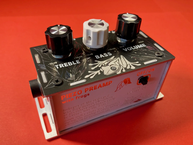
Piezo Preamp v3.1
Github repository for the preamp is here.
Github repository for the enclosure is here.
Motivation & inspiration
I made this project for two reasons: to finally learn proper PCB design and to be able to plug my kantele into my guitar pedals. Learning PCB design emerged simply as a necessity - I was working mainly with stripboard before and the level of messiness became quickly unmanageable. As for the second reason - kantele is a simple acoustic stringed instrument from Finland. I bought a cheap one and wanted to capture its sound and postprocess it. This led me to piezo microphones and subsequently to piezo preamps.
On piezo microphones
Also called "contact microphones", these small devices are attached to the body of an acoustic instrument. They transform mechanical vibrations into electric charge by means of a property called piezoelectricity. You can buy ready-made microphones of various prices and quality, or make your own from piezo discs (readily available on Mouser etc), bottle caps, wire, glue and a bit of soldering.
A basic model of a piezo microphone is this:

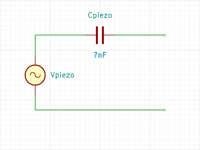
Simple piezoelectric microphone model. High output impedance!
The capacitance in series with the voltage source is in the range of nanofarads. In my measurements, piezo discs had the following capacitances:
- small disc (15mm diameter): ~7-10nF
- medium disc (27mm diameter): ~16-22nF
- large disc (35mm diameter): ~37-40nF
This also means the output impedance can be very high. That is the reason why these microphones are often followed by piezo preamps, which can handle the microphone's output impedance in the full audio frequency range.
It's important to know that piezo discs have a certain resonance frequency at which their frequency response peaks. This frequency differs from manufacturer to manufacturer, from one disc size to another and between individual discs of the same type, but some examples from specifications are:
- 1.3±0.5kHz for Murata 7NB-31R2-1, 31mm, nickel alloy
- 2.6±0.5kHz for Same Sky (formerly CUI) CPT-3526-L100, 35mm, brass
- 4.6±0.5kHz for Same Sky CPT-2746-L100, 27mm, brass.
The frequency characteristic is further affected by the body (shell) of the microphone itself, the mass of the body of the acoustic instruments onto which the microphone is attached and by the position of the microphone on the instrument. Finding the best-sounding spot on the body of the instrument is often a matter of trial and error. A piezo preamp might also try to provide means by which the tone can be further adjusted.
On piezo preamps
When designing a piezo preamp, we basically have two options. The classic and common approach is to use a circuit with very high input impedance - much higher than the output impedance of the microphone. For that purpose, you'll probably end up using JFETs, FET-input opamps or bootstrapping. The other approach is to use a so-called charge amplifier. This is a simple circuit with somehow counterintuitive low input impedance, and apparently it's not very common in the audio electronics world.
Charge amplifier
Low input impedance gives the circuit certain advantages, namely:
- the capacitance of the cable between the microphone and the preamp (which is modeled by a capacitor in parallel to the microphone's output) has no effect on the frequency response of the circuit.
- the triboelectric effect of the cable is reduced - that's the noise produced by the cable when it moves.
- 50/60Hz mains hum pickup should be reduced.
Let's look at the basic charge amplifier circuit:

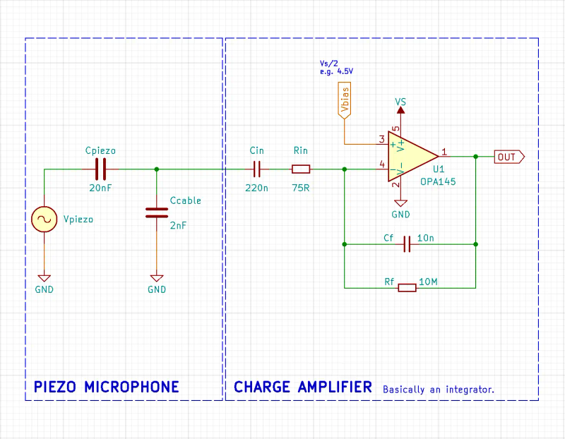
Piezo mic connected to a basic charge amplifier.
The OPA145 opamp on the picture is not specific for charge amplifiers, just the one I chose for my preamp (more on this later), and should be of FET-input type. It's in the inverting configuration, hence the low input impedance. The circuit is basically an integrator, but the signal from the piezo microphone passes the piezo capacitance Cpiezo in series, which works as a differentiator, so the two effects cancel each other out.
An important component of the charge amp is the capacitor in the opamp's feedback loop. The ratio of the piezo capacitance and the feedback capacitance sets the gain, so for Cpiezo = 20nF and Cf = 10nF, the gain is 2. If we want to change the gain of the circuit, we need to change the feedback capacitance.
Choosing the opamp
I chose OPA145 because it has:
- JFET input stage, which means low input bias and offset current - critical for a charge amplifier
- acceptable input voltage noise density of 7nV/rtHz
- good current noise density of 0.8fA/rtHz
- slew rate of 20V/us - above the 2.3V/us recommended for audio by Douglas Self
- GBW of 5.5MHz - above the 3MHz recommended for audio
- single supply voltage range of 4.5V - 36V
- output voltage swing of (V- +0.3, V+ -0.3)
- exceptionally low max quiescent current of 0.655mA, ensuring long battery life
- a reasonable price.
OPA145 also unfortunately seems to have bias current cancellation, which might introduce more current noise. I chose two single OPA145 packages instead of a dual OPA2145 because they are much easier to route and the crosstalk and power dissipation are minimized (less heat). This increases the price, of course.
Block diagram

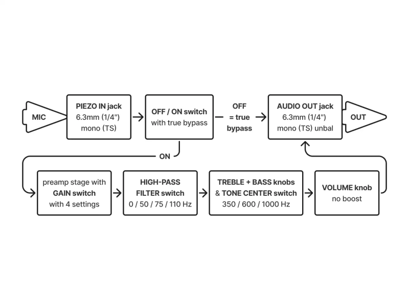
Piezo preamp block diagram.
The piezo mic goes into the PIEZO IN 6.3" mono TS jack, followed by the ON/OFF switch with the OFF position being the true bypass. The charge amplifier follows. Its gain can be changed using the GAIN switch. The signal then goes to the passive high-pass filter (HPF switch) and active Baxandall tone control (BASS and TREBLE knobs) with switchable tone center (CENTER switch, see the images below). A simple passive VOLUME knob follows, and the chain ends in the 6.3" mono TS AUDIO OUT jack.

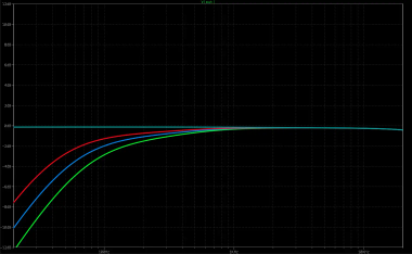

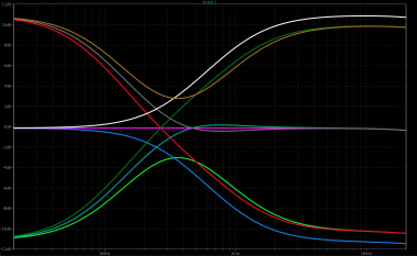

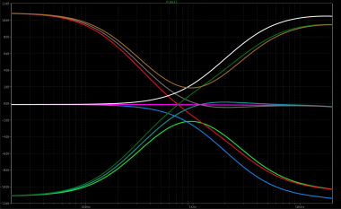
- High-pass filter operation modes - 0, 50, 75 and 110 Hz.
- Baxandall tone control - centered at 350 Hz.
- Baxandall tone control - centered at 1000 Hz. Switched by the CENTER switch.
Main schematics

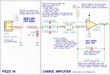

- Charge amplifier. GAIN switch swaps feedback caps (not shown).
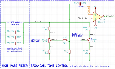
- High-pass filter + Baxandall tone control. HPF switch and CENTER switch swap filter and bass/treble caps (not shown).
The KiCad project is available in the project repository here. See schematics/ folder for the exported images of the full schematics.
The GAIN switch swaps the feedback capacitors, providing these four values: 1nF, 5.7nF, 10.4nF and 23nF.
The HPF is just a switched capacitor bank, forming simple first-order HPF with cutoff frequencies of 0, 50, 75 and 110 Hz.
The Baxandall circuit is pretty standard, providing BASS and TREBLE pots, utilizing low-value resistors for less Johnson noise and operating on +-10dB. Switching of the center frequency (350 / 600 / 1000 Hz) is achieved by the swapping of the values of the bass and treble capacitors with the CENTER switch.
Additional subcircuits
For the proper and convenient operation of the preamp, we need a few additional bells and whistles.
Battery / DC switching

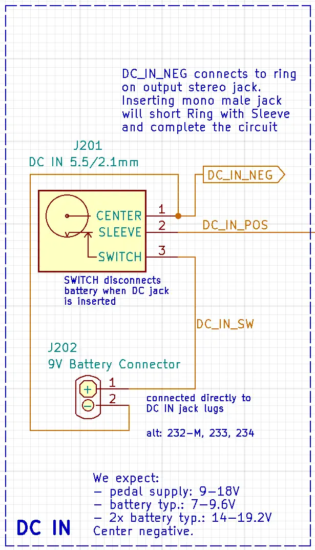
DC input jack with battery switch.
The input DC jack is a 3-pin component with a switch which disconnects the battery connector J202 when the DC connector is inserted.
ESD / EOS protection

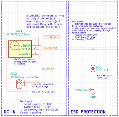

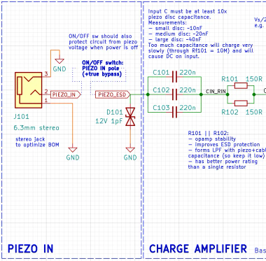

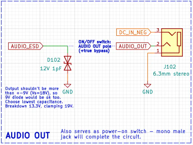
- TVS diode D201 (D20V0L1B2WS-7) on DC input.
- TVS diode D101 (CDSOD323-T12LC) and R101 || R102 on piezo microphone input.
- TVS diode D102 (CDSOD323-T12LC) on audio output.
The DC input is protected by D201 TVS diode, a D20V0L1B2WS-7 with 20V reverse standoff. The preamp is intended to work with 9V batteries, but the circuit was designed to theoretically handle DC 18V to allow for more headroom, that's why the 20V TVS is used.
The input piezo jack and output audio jack are both protected by CDSOD323-T12LC TVS (D101, D102) with 12V reverse standoff. They were chosen specifically for their low capacitance of 1pF, which is important mainly for the charge amplifier.
The charge amplifier's input resistors R101 || R102 help limit the maximum current during electrical overstress, admittedly not to a great extent. OPA145 contains internal ESD protection circuitry, but this shouldn't be relied upon as the sole protective measure.
Battery indicator circuit

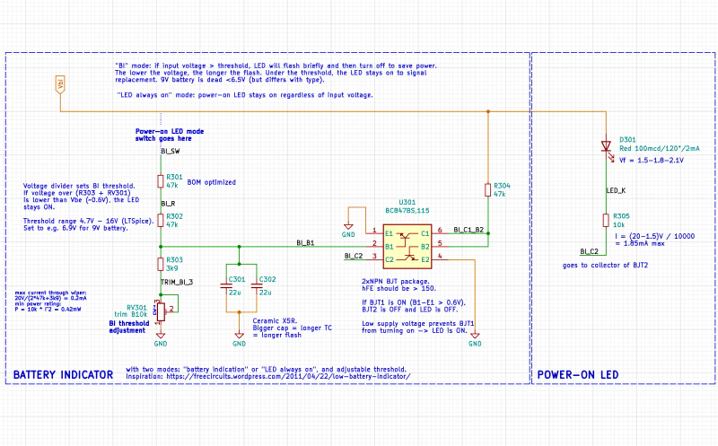
Battery indicator. LED mode switch is a simple SPDT (not shown).
Since the preamp can be powered by a 9V battery, and nothing is more inconvenient than discovering that your battery has died in the middle of your concert, we need a simple way to indicate that the battery needs replacing.
When the power is turned on, the presented circuit will turn the D301 LED on at first. After the C301 + C302 caps charge, the base B1 of U301 (dual BJT package) achieves the Vbe voltage (e.g. 0.6V). The transistor 1 will start to conduct, which will pull the base B2 of transistor 2 down to GND. This will turn the second transistor and the LED (grounded through C2 - E2) off.
The lower the input voltage, the longer the D301 stays on, because the capacitors charge more slowly. Under a certain threshold input voltage, the base of transistor 1 will never achieve the sufficient Vbe to turn the transistor 1 on, and the LED will stay on indefinitely, indicating the battery should be replaced. The exact value of the threshold voltage is set by a resistor divider formed by R301 + R302 and R303 + RV301. RV301 is a trimmer, so the threshold voltage can (and should) be set manually during the assembly to some reasonable level, e.g. 6.9V. This value also depends on the battery type.
S301 is a simple SPDT switch which turns this whole subcircuit off, effectively forcing the LED stay on all the time. This is useful for the operation of the preamp with normal pedal-style DC input, i.e. without the battery.
Reverse polarity protection

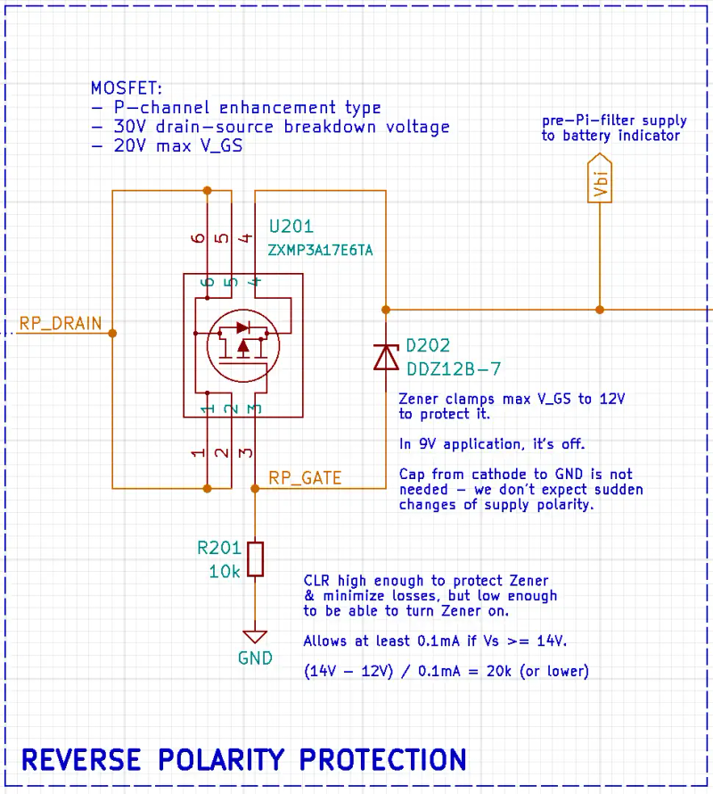
Reverse polarity protection based on a P-channel MOSFET.
The circuit is based on a P-channel enhancement mode MOSFET. When the polarity is reversed (i.e. GND becomes the supply voltage and RP_DRAIN becomes the ground), the gate of the MOSFET turns the transistor off, effectively creating an open circuit. This is better than the usual diode in series (which would cause a voltage drop) or the diode in parallel (which would cause a short circuit if the polarity is reversed, leaving the DC supply to deal with it 😎).
Power supply filtering


Pi filter for power supply.
A simple Pi filter with the cutoff of 72Hz. See Phil's lab #74 for more info.
Opamp biasing

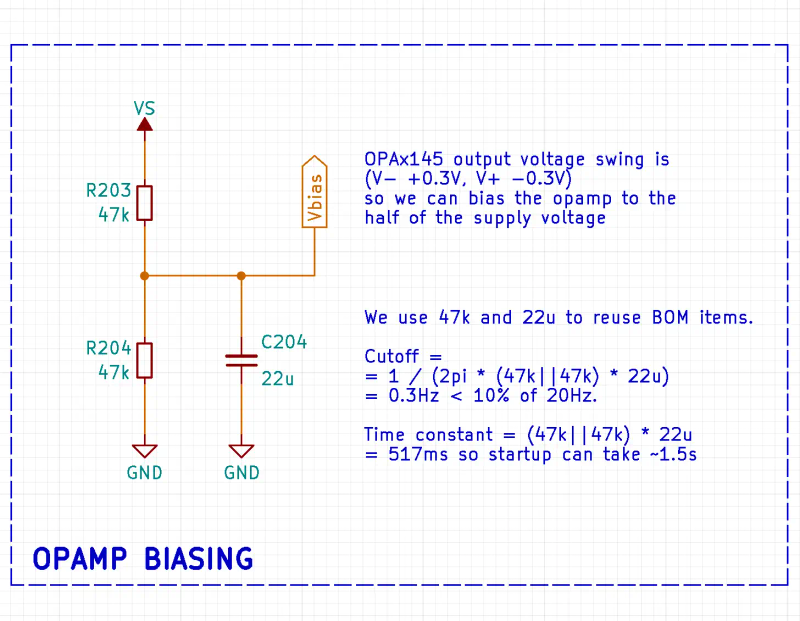
Generating bias voltage for opamps.
The voltage source is unipolar, thus we need this simple biasing circuit with cutoff of 0.3Hz and the time constant of 517ms. The startup can take ~1.5s.
Simulations in LTSpice
The simulations files are available in the project repo here.
AC analysis of the charge amplifier itself
File name: simulation-charge_amp_only.asc

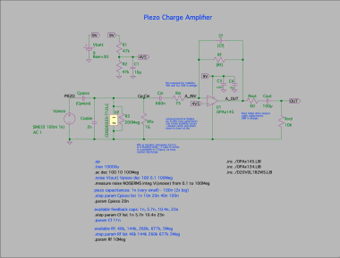

- AC analysis of the charge amp itself - LTSpice file.
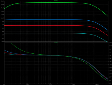
- AC analysis of the charge amp itself. Cpiezo = 20nF, traces from top: Cf = 1nF (gain = 20), Cf = 5.7nF (gain = 3.5), Cf = 10.4nF (gain = 1.92), Cf = 23nF (gain = 0.87).
We're looking at the frequency response of the charge amp alone. Piezo mic capacitance is fixed at 20nF and the feedback cap (determining the charge amplifier's gain) steps through 4 implemented values of 1nF, 5.7nF, 10.4nF and 23nF. The frequency response has the -3dB point well beyond 20kHz - this will be further limited by the next stages.
Stability analysis of the charge amplifier itself
File name: stability-charge_amp_only.asc

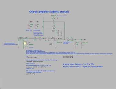

- Stability of the charge amp itself - LTSpice file.
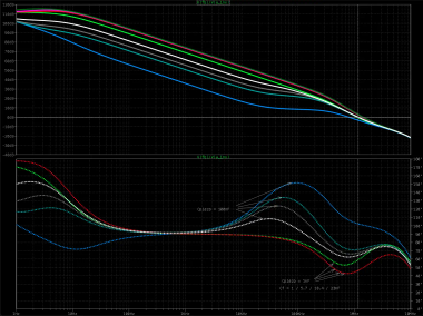
- Stability of the charge amp iself. Cpiezo = 1 / 100nF, Cf = 1 / 5.7 / 10.4 / 23 nF.
The plots display the loop gain of the charge amplifier itself. Phase margin (determining the opamp's stability) is the phase (bottom pane) where the traces in the top pane cross the 0dB threshold. Two different piezo mic capacitances are simulated: 1nF and 100nF; and our four feedback capacitor values, so we should see 8 traces in total - but the phase traces in the bottom pane are overlapping for Cpiezo = 1nF, that's why only 6 traces are visible.
We see that the worst case for stability is Cpiezo = 1nF and Cf = 23nF, i.e. gain of 0.04. The phase margin gets dangerously close to 45°, which is generally considered to be only "marginally stable". Manufacturing differences between individual opamps of the same model (aka "process variation") may make this ultra low-gain configuration unstable. Adding HPF + Baxandall as the next stages seems to improve the stability, though.
AC analysis of the charge amp + HPF + Baxandall tone control
File name: simulation-charge_amp+bax.asc

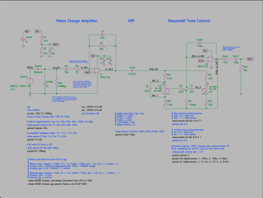

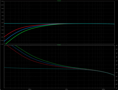

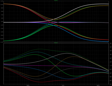
- AC analysis of the charge amp + HPF + Baxandall - LTSpice file.
- AC analysis of the HPF - cutoffs of 0 / 50 / 77 / 113 Hz.
- AC analysis of the Baxandall tone control. Cpiezo = 23nF, Cf = 23nF, gain = 1, center = 600Hz.
Operation of the HPF and the Baxandall with the center of 600Hz is shown (+-10dB).
Stability analysis of the charge amp + HPF + Baxandall tone control
File name: stability-charge_amp+baxandall.asc

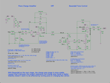

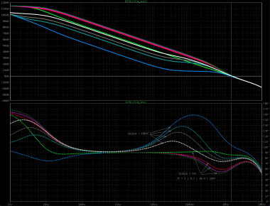
- Stability of the charge amp + HPF + Bax - LTSpice file.
- Stability of the charge amp + HPF + Bax. Cpiezo = 1 / 100nF, Cf = 1 / 5.7 / 10.4 / 23 nF.
Again, the loop gain and phase margin is shown with Cpiezo = 1 / 100nF and our four feedback caps. It seems that adding HPF and Baxandall stages after the charge amplifier improves the stability even in the worst case scenario (Cpiezo = 1nF, Cf = 23nF). I guess this might be attributed to the charge amp feeding higher resistance now. The stability doesn't seem to be affected by the changing of the Baxandall tone center or turning of the BASS / TREBLE pots.
AC analysis of the power supply Pi filter
File name: simulation-pi_filter.asc


- AC analysis of the Pi filter - LTSpice file.
- AC analysis of the Pi filter - frequency response. Cutoff is at 72Hz.
Transient analysis of the battery indicator circuit
File name: simulation-battery_indicator.asc

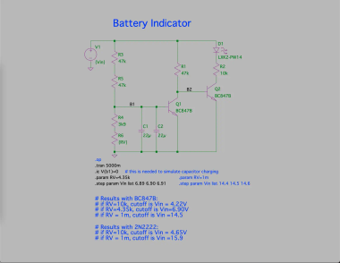

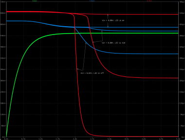
- AC analysis of the battery indicator - LTSpice file.
- AC analysis of the battery indicator. With trimmer R6 at 4.35kHz, the threshold is at 6.90V.
We set the R6 (trimmer RV301 in KiCad schematic) to 4.35kOhm and step the input voltage through 6.89 / 6.90 / 6.91 Volts. We see that at 6.89V, the I(D1), i.e. the current through the LED diode, is 440uA and the voltage at the base of the second BJT V(b2) is just below the 600mV. The Vbe base-emitter threshold voltage for the BC847B is 580 - 700mV. The transistor is on and the LED is on too. With input voltage of 6.91, the V(b2) drops to 440mV which is too low and the current through the LED drops to 0. This means that if we want to setup the battery indicator so that the LED shines when the battery is below 6.90V, we should set the trimmer to 4.35kOhm. In practice the exact value of the trimmer will depend on the characteristics of the individual transistors at hand - that's why the trimmer has been provided.
The trimmer allows for the threshold to be set in the range of 4.2V to 14.5V - useful for powering from two 9V batteries in series, though I'm not sure how would anyone connect them physically.
OPA145 noise analysis
File name: noise-opamp.asc

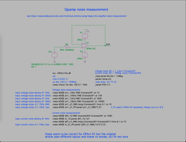


- OPA145 noise analysis - LTSpice file.
- OPA145 noise analysis.
An attempt at simulating voltage and current noise of OPA145. Further measurements are in the LTSpice log file.
An attempt to analyse electrical overstress (EOS)
File name: EOS_attempt-charge_amp_only.asc
Not a good attempt though, I guess :). This simulation is unfinished.
First prototypes - v1 & v2

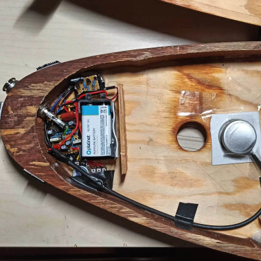

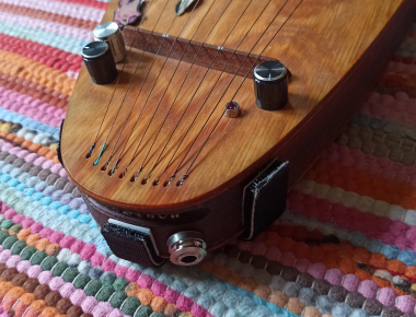
- Preamp v1 - on stripboard, installed directly in the kantele.
- Preamp v1 - top side of the instrument.
The preamp v1 was created on a stripboard and installed directly into the kantele (a cheap one, don't worry), omitting a few subcircuits. Admittedly kinda sketchy, but it worked well.

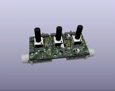

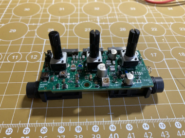

- Preamp v2 - PCB render from KiCad.
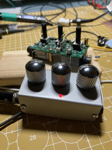
- Preamp v2 - manufactured and assembled PCB.
- Preamp v2 - in self-drilled enclosure.
The second version is standalone and was built on a 4-layer PCB. This project lives in its own repository here. I also designed an enclosure from PCBs (more on this later), mainly to learn Altium a bit - it's available here, but be warned, I haven't tried sending it off for manufacturing at all.
PCB design - v3

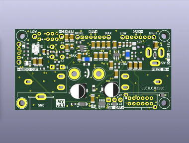



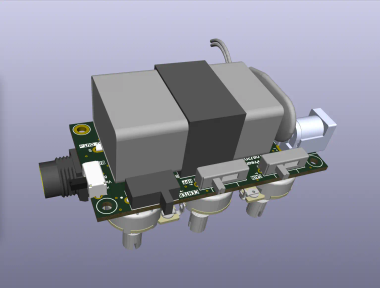

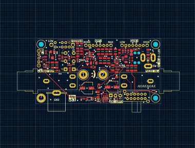


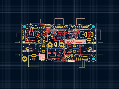
- Preamp v3 - PCB render, top side, SMD components only.
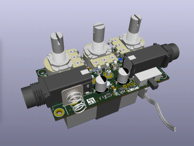
- Preamp v3 - PCB render, top side, SMD + THT components.
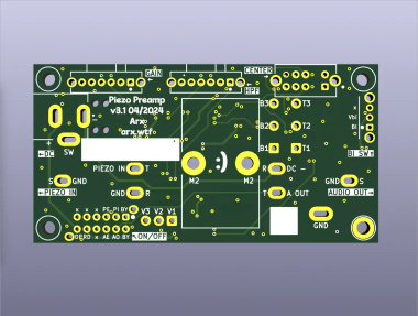
- Preamp v3 - PCB render, bottom side, SMD components only (yes, none).
- Preamp v3 - PCB render, bottom side, THT components and battery.
- Preamp v3 - PCB design, top side.
- Preamp v3 - PCB design, bottom side.
- Preamp v3 - PCB design, both sides.
The PCB was created in KiCad v8 and it's a 4-layer PCB with Signal - GND - GND - Signal stackup, recommended in the famous Rick Hartley video. To save board space, the pots have to be mounted on the panel, not on the PCB, which adds some extra work during the assembly. The battery holder is mounted from the bottom side. I chose the SMD technology to again save some board space and manual assembly time :). The final boards were manufactured and assembled by JLCPCB.
Enclosure from ALU PCBs

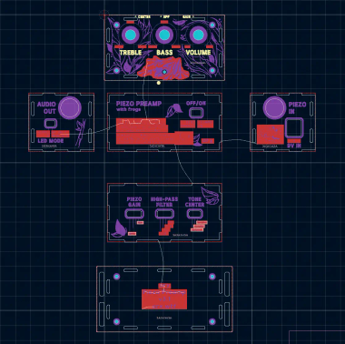

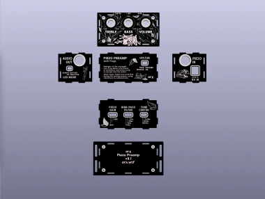
- Enclosure for preamp v3 - multi-board project using KiKit.
- Enclosure for preamp v3 - render from KiCad.
Since drilling ready-made enclosures is laborious and often imprecise, I decided to assemble a simple enclosure from six individual pieces of aluminum PCBs. I previously wrote some tips about this process here.
Using PCBs allowed me to include all the texts, markings and some artworks too. The individual sides of the enclosure fit together. The four large oval cutouts on the bottom plate allow for mounting of the preamp to a pedalboard or to a guitar strap with the help of e.g. cable ties.
I chose aluminum PCBs instead of the classic FR4 for the better shielding of the circuit from electromagnetism. The enclosure is grounded to the main PCB in a single point - a battery spring "misused" for this purpose, located near the output jack. If needed, it can also be grounded by using metal PCB standoffs in the lower left corner of the board.
The enclosure project for v3 is available in this repository and was created as a KiCad v8 project with the help of KiKit - a plugin that allows the design of all of the sides in one multi-board project. Also manufactured by JLCPCB.
Final product

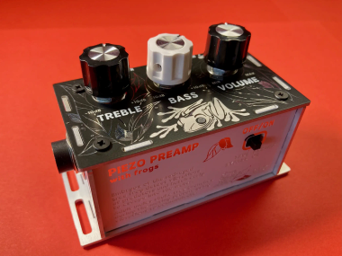

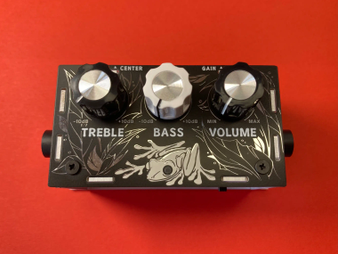

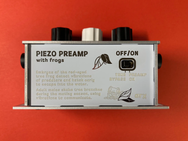

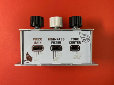


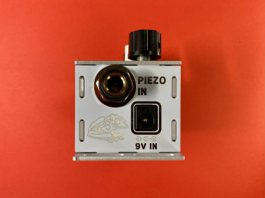

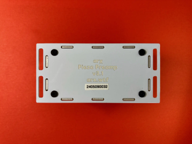

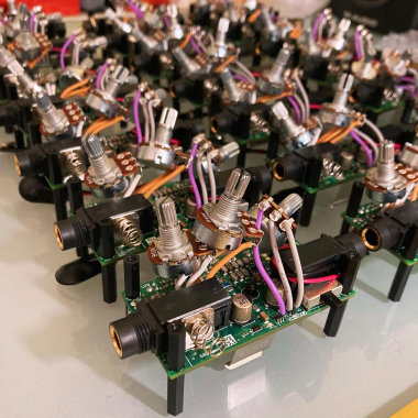
- Piezo Preamp v3.
- Piezo Preamp v3 - top side.
- Piezo Preamp v3 - front side.
- Piezo Preamp v3 - back side.
- Piezo Preamp v3 - left side.
- Piezo Preamp v3 - right side.
- Piezo Preamp v3 - bottom side.
- Piezo Preamp v3 - assembly.
BOM costs
I manufactured about 20 pieces of the preamp. At the time of assembly (2024), the costs per one preamp were those in the table below. I used some discount JLC coupon for fab and SMD assembly - they distribute those frequently.
| Item | Per 1 preamp |
|---|---|
| PCB fab + SMD components + assembly | $15.25 |
| PCB shipping to EU | $1.34 |
| PCB duties + VAT | $4.35 |
| THT components (jacks, pots etc) | $10.99 |
| Enclosure fab - all 6 sides | $3.10 |
| Enclosure shipping to EU | $1.37 |
| Enclosure duties + VAT | $0.94 |
| Nuts, bolts, washers, standoffs | $1.21 |
| Knobs | $1.88 |
| Total | $40.43 |
Of course, ordering just 3 pieces (or whatever the minimum JLC order quantity is) would probably cost much more.
Product performance
The preamp works as intended! :).
The typical current consumption is less than 2mA.
I performed some prelimary testing using REW, an excellent free tool for audio gear and room measurements, to confirm that all the user controls work as intended. Unfortunately, my current sound interface does not provide sufficient capabilities for truly precise measurements.
I'll expand this section once I've acquired better hardware tools (DAC, ADC) for the measurements.