Using PCBs to create front panels for your projects
Regular FR4 or aluminum PCBs can be used to create cheap (but beautiful) front panels for electronic projects. In this article, we'll explore various tips & techniques used to obtain the best results.

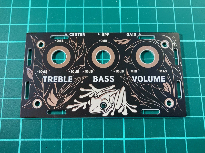
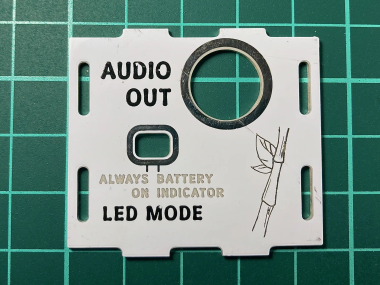
Example of an aluminum front panel. Black solder mask, white silkscreen (text), creamy dielectric on core (the frog) and silver HASL finish (the leaves).
It wouldn't be possible to compile these tips without reading through this massive thread on ModWiggler first. Huge thanks goes to everyone who contributed to the thread!
I personally use Kicad and JLCPCB to create my front panels. However, these tips are pretty universal and should apply to other CAD softwares and fab houses as well.
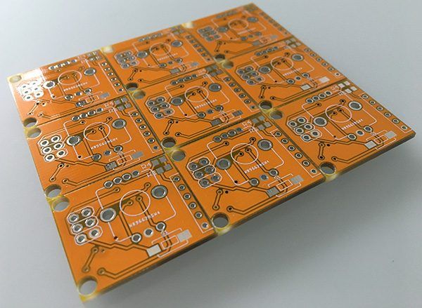
The test PCB
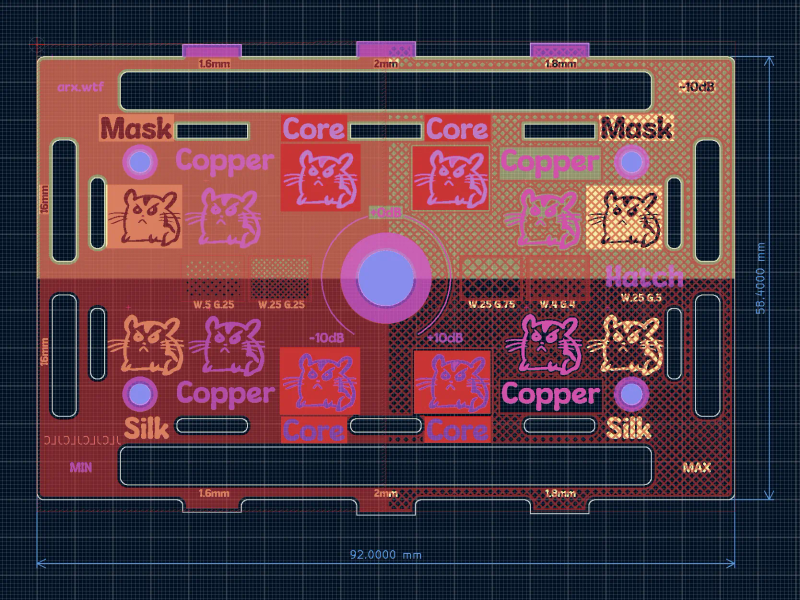
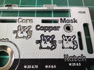
A PCB to test the capabilities of a fab house.
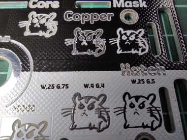
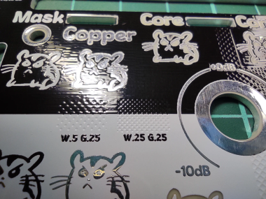
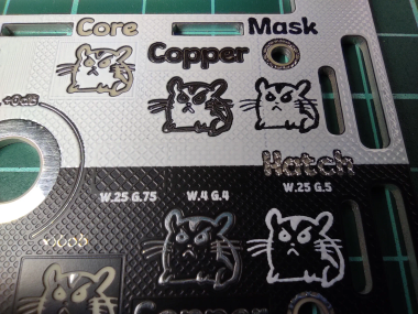
In order to test the capabilities of a fab house and demonstrate the points in this article, I created a PCB using various techniques. The bottom half of the board has the solder mask as the "background color" and shows the text and graphics on the silkscreen, on copper (HASL) and core. On the top half, the background is done by a continuous silkscreen fill, and the text and graphics are done on solder mask (an opening in silkscreen fill), copper and core.
Furthermore, the left half of the PCB has a solid copper fill; the right half has a cross-hatched copper fill. Smaller rectangular regions of different cross-hatch parameters (hatch width and gap) are present in the middle as well.
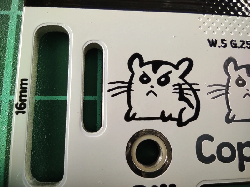
The PCB contains 4 smaller mounting holes (which are drilled), one big hole (which needs to be routed) and cutouts and ovals of various sizes (which are routed as well). The three top inner cutouts are rectangular with 90-degree angles - which technically isn't possible with JLCPCB. The three top-most protrusions on the outer board edge have 90-degree angles as well. The three bottom cutouts and the protrusions on the outer edge have the border radius of 0.8mm.
The project is available on my Github - you are free to use the gerbers or adjust the PCB to your needs first. If you happen to test the capabilities of a fab house, feel free to send me the pictures to arx@synth.sk!
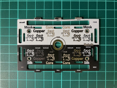
I had this board manufactured by JLCPCB in two versions: one with white solder mask and black silkscreen, the other with black matte solder mask and white silkscreen. The core is aluminum. Here are the results. All the images are clickable and the grid on the background is in centimeters.
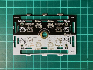
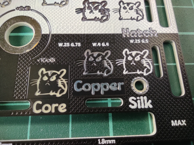
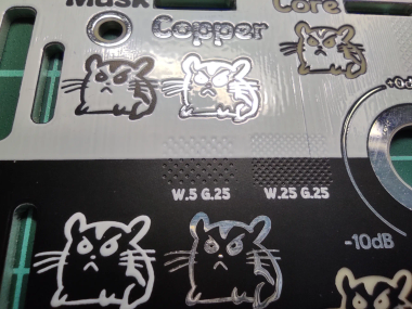
- Test PCB - white solder mask, black silkscreen, HASL finish, creamy ALU core dielectric
- Test PCB - black solder mask, white silkscreen, HASL finish, creamy ALU core dielectric
1. Fab house capabilities and communication
Since no two PCB manufacturers (fab houses) have the same processes, this is the prerequisite for all the other tips. Study the fab house capabilities on their website. These can also change from time to time, so it's better to check before every order. Ask their customer support about their processes before ordering, or be prepared to iterate. Search the internet for examples of previously finished panels. Communicate all your intentions clearly in the order notes. Tell them this is a front panel, not a standard electrical circuit, so they don't have to search for electrical errors.
A note on the word "panels": manufacturers also use this word for the process of panelizing multiple PCBs into one bigger PCB (see tip #4). Keep this in mind and use "front panels" or "faceplate" in communication.
2. Choose the right software tools
For PCB design, some use Kicad, others EasyEDA (JLCPCB's tool), others Eagle or Altium. There are countless other choices, some free, some paid. Simple panels with text and basic shapes can be done directly in Kicad or EasyEDA for free.
For creating advanced artworks, use vector graphic editors like Inkscape (free) or Adobe Illustrator (paid). Exporting the artwork in DXF makes it easier to import to Kicad. Kicad also includes Image Converter for importing other (non-vector) types of graphics.
3. Consider the size of your front panel
This generally depends on the enclosure you'll be using for your finished project. Different fab houses can handle different maximum sizes, or have different tiers of service for different sizes of boards. In JLCPCB, keeping the total size of your boards under 100x100mm will get you the cheapest price.
4. Consider panelizing your...front panels
In PCB manufacturing world, panelizing is the process of repeating the same PCB design on one physical board multiple times, or using different designs next to each other on one physical board. Notice this is a different usage of word "panel" - we're not talking about "front panels" now, but about "collating multiple boards on one PCB panel". The individual boards on a panel are separated by e.g. v-scores or mousebites. These panels are then produced as a single board, which can save you money if you intend to create lots of front panels.
PCB panelizing with v-scores. Image by Mauro Alfieri, CC BY-NC-SA 4.0, no changes
The fab houses have different panelizing abilities. JLC can panelize your boards for you, if you indicate it in their order form - for a fee, and the individual boards must be rectangular. Or you can panelize them yourself, see Kikit plugin for Kicad. You will have to study your fab house requirements and recommendations to successfully create a panel of PCBs.
Keep in mind that the process of de-panelizing of individual boards from the panel can leave marks and rough edges on the finished boards.
5. Choose the PCB core material
Two most common choices are 2-layer FR4 (fiberglass - classic PCB material) and 1-layer (single-sided) aluminum.
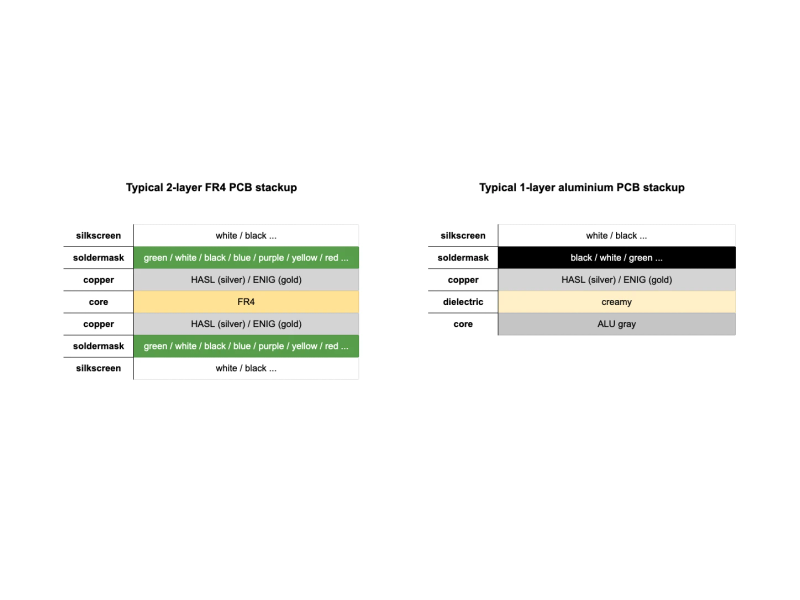
Comparison of stackups for 2-layer FR4 and 1-layer ALU PCB
About FR4 front panels
- FR4 is less rigid - it might bend considerably if, for example, your users are going to insert jacks into huge panels. The panel can crack or the fibers can start falling off from the sides of the panel. Consider sealing the sides of your board with some polyurethane or acrylic product, or shellac (but don't clean it with alcohol afterwards).
- You can work with both sides of the board. If you leave out copper and solder mask in certain areas on both sides of the board, you can achieve certain level of transparency of the panel and use this together with an LED for nice effects.
- The copper fills (on both sides!) also affect the color of the solder mask on your front panel.
- You can use different designs on the front and back side of the board. This can be used to add easter eggs to the back, serial numbers, additional info or whatever. Or your users can choose which side they prefer (if your panel is symmetrical and can be flipped, that is).
- You can mount SMD packages on both sides of the panel. You can use through-hole components too.
- You can design touch controls by using traces, vias, and an SMD connector on the back side.
- The panel can be grounded by using copper fills and connecting the fill to ground on your main PCB somehow (with a via and a connector on back?).
About aluminum front panels
- It's more rigid, less prone to bends and cracks.
- You can usually work on one side of the board only (fab limitation), or it might be the cheaper option.
- The core ALU material has no transparency. Using a copper fill on the back side (in case you order two-sided ALU board) will not affect the looks of the front side.
- You can't use SMDs on the back (if it is a one-sided board). Through-hole components won't work if the holes are not individually insulated, which is expensive. The PCB core is conductive, so you'll end up with lots of electrical shorts.
- The panel can be grounded by connecting it to ground on your main PCB, for example by using a battery contact with a spring touching the back side of the panel. Sand down any protective layers on the back side of the panel first.
- You can still design touch controls by using traces, but connecting them back to your main circuit PCB might be problematic - you can't use a via and an SMD connector on the back.
- It's generally more expensive.
- Minimum size of the drill used for routing might be larger, limiting the border radius of your cutouts.
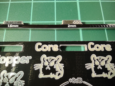
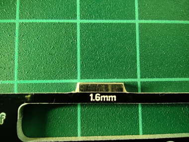
6. Board thickness and rigidity
The standard PCB thickness is 1.6mm. Sometimes you might want to choose more (2mm), especially for larger FR4 boards with large female jacks. This will probably increase the cost and affect the transparency of the board.
Using copper fills on both sides of FR4 boards can improve their rigidity. Mounting another regular PCB in parallel behind the front panel with jacks and standoffs connecting the panel to the second PCB can also help. Bolting two identical panels together (e.g. with jacks coming through both of them) will help, but the jacks must have sufficiently long bushings.
7. Color combinations
This is your color palette:
- Silkscreen color: usually black or white. This is the top-most layer, printed on solder mask. It can also be printed directly on core, but that might peel off easily. Can also be used for large silkscreen fills, which can lead to uneven surface and "streaks" of silkscreen color.
- solder mask color: black, matte black, white, green, red, yellow, blue, etc. Standard is green, any other color will probably be more expensive. Keep in mind that the color of the solder mask is usually different (brighter) if there is copper underneath it. With FR4 boards, the presence of copper and solder mask on the other side of the board can also change the solder mask color, because of core transparency. Matte colors are usually more expensive and might collect fingerprint marks more easily, especially on black solder mask.
- Color of exposed copper - traces, pads and fills. These will be visible if you leave a solder mask opening above them. It can either be plain copper (which is unstable), gold (ENIG finish) or silvery color (HASL).
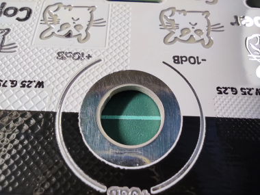
- Color of the exposed core: yellow-ish with FR4, creamy with ALU on the front side (actually a dielectric layer on ALU core) or the color of aluminum on the back side of ALU PCB. You'll only see this color if there is no copper and no solder mask on top of the core. With FR4, presence of copper and solder mask on the back side changes this color because of core transparency.
Colors of white solder mask test PCB
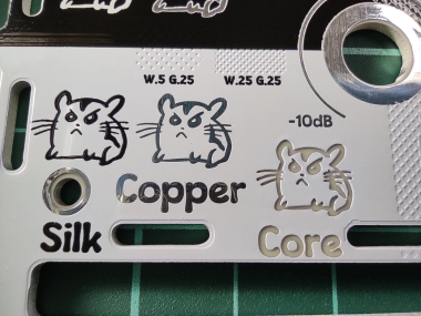
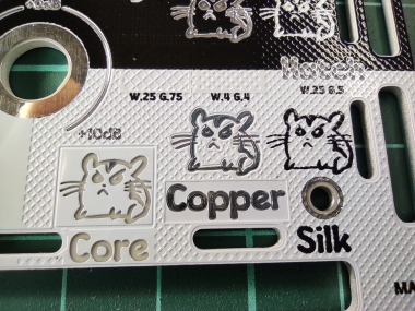
- White solder mask, black silkscreen, solid copper fill, HASL finish, ALU core
- White solder mask, black silkscreen fill (notice the poor surface quality), solid copper fill, HASL finish, ALU core
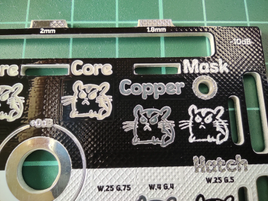
- White solder mask, black silkscreen, cross-hatched copper fill, HASL finish, ALU core
- White solder mask, black silkscreen fill on top of cross-hatched copper fill, HASL finish, ALU core
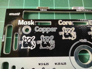
Colors of black solder mask test PCB
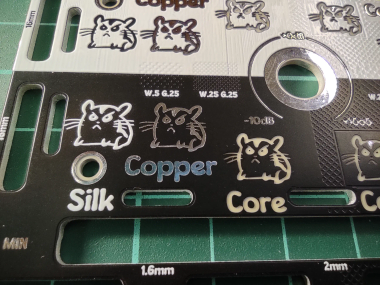
- Matte black solder mask, white silkscreen, solid copper fill, HASL finish, ALU core
- Matte black solder mask, white silkscreen fill (notice the poor surface quality), solid copper fill, HASL finish, ALU core
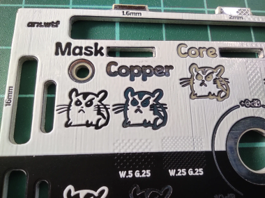
- Matte black solder mask, white silkscreen, cross-hatched copper fill, HASL finish, ALU core
- Matte black solder mask, white silkscreen fill on top of cross-hatched copper fill, HASL finish, ALU core

The frog is creamy dielectric on core with copper outlines (HASL). Black matte solder mask, white silkscreen.
I also recommend this Reddit thread to see more examples of the color combinations on FR4 boards.
8. Copper finish
Some fab houses will allow you tu use raw, unfinished copper on traces and fills. This is unstable and will change its color with time and finger touches.
Two most common copper finishes are ENIG (gold) and HASL (silver). You can't use both of them on the same board.
ENIG (Electroless Nickel Immersion Gold) usually looks more professional and smooth. HASL (Hot Air Solder Leveling) can be uneven and prone to scratches. Use lead-free HASL (which is usually more expensive), since user will be able to touch it and lead is toxic.
HASL vs ENIG
- HASL finish. ALU board, white solder mask, black silkscreen. Notice the scratches.
- ENIG finish. FR4 board, black solder mask, white silkscreen.
9. Artwork resolution
Silkscreen usually is the least precise. Expect printing errors, possibly production smears etc. Depending on the fab process, the silkscreen might start to peel off with usage. As such, it's best to use it for non-critical accents in the artwork and text (watch out for minimum text size capability). Printing silkscreen directly on core is not recommended - it's easy to scratch off, especially on ALU PCBs.
Traces and solder mask openings are usually much more precise. If you want to "write text" or shapes with copper, use a copper fill and expose the solder mask in the desired shapes. If you don't want to use a copper fill, the copper traces can have exactly the same shape as solder mask openings, but expect imperfections.
Keep in mind that with solder mask openings, you can create a precise image or text directly on the core (or the core dielectric in case of the ALU core), if there's no copper on top of the core. Such openings will be visibly under the level of the solder mask. See the picture of frog in tip #7.
As for the artworks themselves - google "pcb art" and be impressed.
10. Texture and smoothness
It's recommended to use copper fills under solder mask to make it more smooth and hide any imperfection of the core. This will make the solder mask color brighter, though, and will leave a small border on the edges of the board and holes / cutouts, since the copper fill can't reach right up to the edge. Check the minimum clearance capability of your fab house, it's usually called copper-to-edge, copper-to-hole, track-to-edge etc.
Notice the (uneven) clearance between the copper fill and the oval cutouts, and on the board edge.
Always expect imperfections and variable quality, especially with large silkscreen fills.
Using cross-hatched copper fills can help against scratches and can look cool. It also makes silkscreen fills look better. You'll have to experiment with hatch widths and spacings (gaps).
Using cross-hatched copper fill
- White solder mask with cross-hatched copper fill. Notice the better-looking black silkscreen fill on top. Different hatch widths and gaps in the middle.
- White solder mask on solid copper fill, and some more cross-hatches in the middle. Poor quality of black silkscreen fill on top.
- Black solder mask with cross-hatched copper fill. Better-looking (but still poor) white silkscreen fill on top. Different hatch widths and gaps in the middle.
- Black solder mask on solid copper fill, and more cross-hatches in the middle. Poor quality of white silkscreen fill on top.
You can also use vias for artistic purposes. Choose between tented (covered by solder mask) or untented vias (exposed, with visible annular ring and the drilling hole).
11. Holes for jacks / pots and cutouts
Check the minimum and maximum hole size the fab house can drill with a regular drill. With JLCPCB, it's 0.3mm - 6.3mm. Include such holes in the drill file with gerbers. Also, check if plated holes (with copper on the inner sides of the hole) will have the diameter specified by you, or the diameter will be decreased by the thickness of plating. The fab house might also have different min and max sizes for plated and unplated holes. Ask the fab house if unsure.
The fab house can also make holes larger than their max drill size, but they will have to be milled (routed) or laser-cut. Check if such larger holes can be plated and if it will cost extra. Large holes should be on edge cuts layer (in Kicad), also called mechanical layer (Altium), .gm1 Protel extension. Routed holes might have rougher edges than simple drilled holes.
Always add some tolerance to hole sizes required for pots and jacks - increase their diameter slightly. For example, use 7.2mm hole for pots with M7 bushing. Check the datasheets of your jacks and potentiometers for any tips on panel hole size.
Oval shapes will always need to be routed as well and may have different min/max capabilities than simple holes.
Rectangular cutouts with sharp precise 90 degree corners might not be manufacturable. Check the minimum inner corner border radius, or ask the fab house what their minimum drill size used for routing is. For example, if the minimum drill size is 1mm, then the minimum border radius is 0.5mm. The drill sizes can be different for FR4 and ALU boards - for JLC (as of 2024), minimum drill size for FR4 is 1mm (border radius of 0.5mm) and for ALU 1.6mm (border radius of 0.8mm). These specs can change.
Imperfections in holes and cutouts

- Imperfectly routed big hole.
- This inner cutout was designed with 90 degree corners, which is not supported by JLCPCB.
- This outer protrusion was also supposed to have 90 degree corners.
- The outer corner, even though defined with a border radius, is also routed imperfectly.
Keep in mind that if you use non-rectangular shapes of your front panel, or add cutouts to the outer edge of your front panels, you will most likely have to panelize the boards yourself - if you want to panelize them (see tip #4).
12. Generating and uploading gerbers, ordering
For generating the output files to be used by your fab house, follow the instructions given by them. They are usually in their FAQ, Knowledge Base or Blog sections of their websites. For example, for Kicad and JLCPCB, use this.
Some fab houses like JLCPCB will print an order number on your front panel (silkscreen). You can specify a placement for this number by using "JLCJLCJLCJLC" text on the silkscreen layer of your board (and indicating it when placing the order). You can place it on the other side of the board, for example - in JLCPCB, this also works for one-sided ALU boards! Or you can ask them to not place the number at all, for a fee. If you forgot and already received boards with the numbers printed on them, you can try carefully removing them with a scalpel and clearcoat the panel afterwards.
The fab house might contact you with additional questions about your boards.
Pay attention to shipping options - sometimes, using the slowest and cheapest option might be better than using a courier service which will force you to pay additional import fees and taxes. For European union, it might be better to use shipping options labeled IOSS / DDP (taxes and import fees paid upfront by the fab house).
With cheap fab houses, always order more front panels than you need. Be prepared to receive boards that have scratches, various defects or marks left by tools the fab house had to use to manufacture the board. PCB manufacturers specialize in manufacturing functional PCBs, NOT artistic front panels. Sometimes you get lucky and most of the boards are usable; other times you can throw half of them away. Some fab houses will accept your complaints, some won't. If possible, use the option to add sheets of paper between individual boards before shipping.
- Scratches, and the silkscreen is already peeling off.
- The color of the core dielectric changed between two batches. The new color is less readable.
There are, of course, specialized front panel manufacturers which offer superior quality - but for a much higher price.
13. After you've received your front panels
You might want to clearcoat your panels to keep them from getting scratched. For panels with granular finish, you can use e.g. Edding E5200 spray for first layers and finish with Altona anti reflection varnish. Using only Altona, you will get smooth surface.
Clearcoating can also hide the scratches made by the fab house.
For better or worse, the fab houses' processes change over time, so don't expect the results to always stay the same.
Closing thoughts
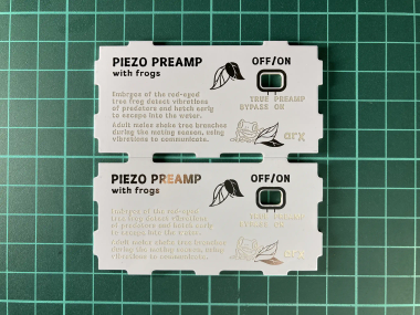
Feel free to send me pictures of your front panels and tell me about your experience! The email is arx@synth.sk. With your permission, I might include the pictures here for future reference of everyone.
These tips were intentionally as general, CAD - agnostic and fab house - agnostic as possible. In my next blog post, I'll give you some more specific tips on using Kicad and JLCPCB. See you there!